1-D ‘wires’ could advance quantum electronics
By Tom Fleischman
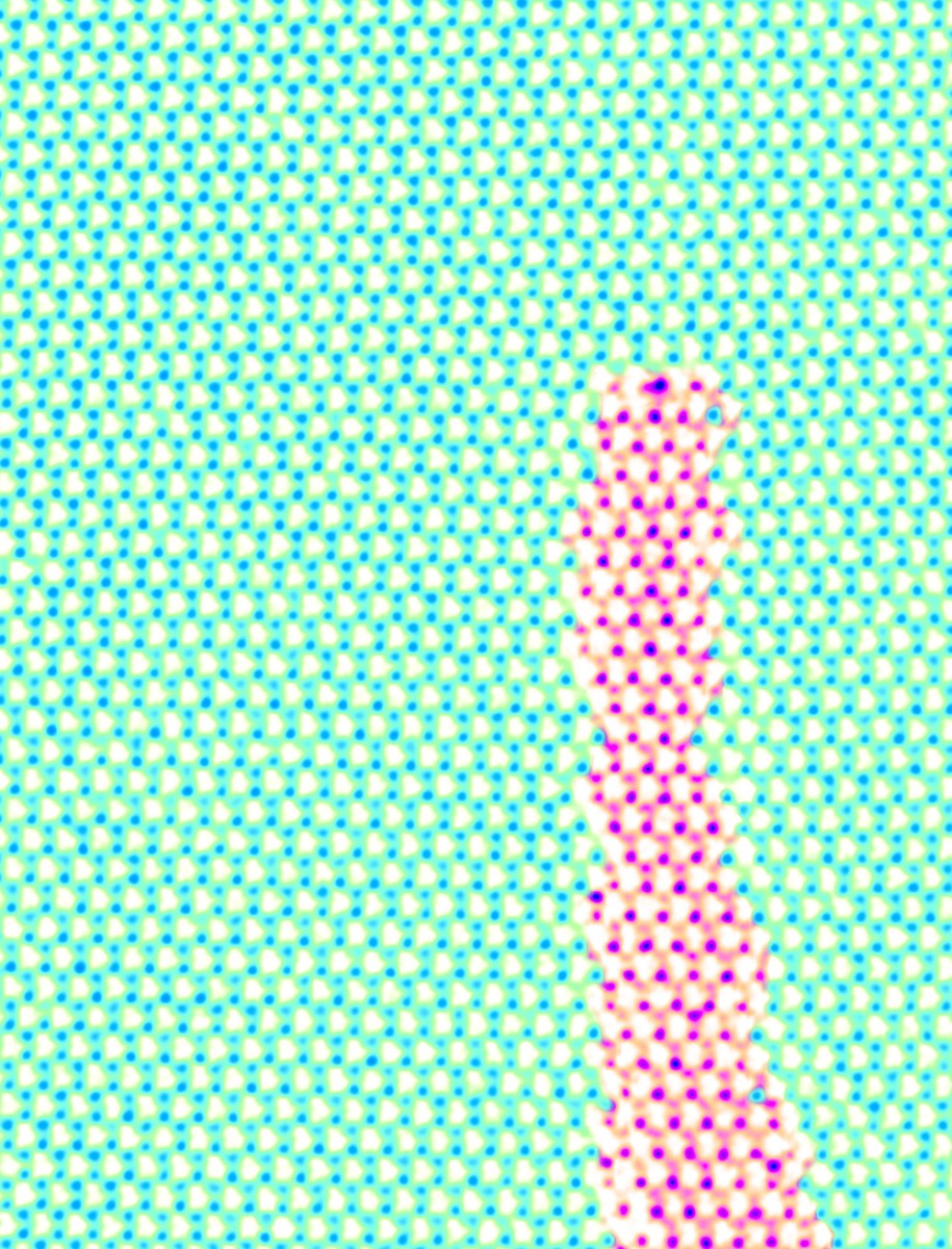
Electron microscope image of a 1-D channel molybdenum disulfide embedded in 2-D tungsten selenide. The blue/green dots are tungsten and selenium atoms; the magenta dots are sulfur atoms. The entire film is three atoms thick.
Materials the thickness of a single atom – known as 2-D materials – hold great promise for next-generation electronics, but actually putting circuitry on something so thin is a challenge.
“If I want to make an atom-sized feature, and I don’t have atom-size control, it’s not going to work,” said David Muller, the Samuel B. Eckert Professor of Engineering in the Department of Applied and Engineering Physics.
Muller and his research collaborators have discovered – a little bit by accident – a method for basically inserting a 1-D semiconductor channel into the “fabric” of a 2-D material. The electronic band structures of these channels exhibit the properties necessary for future electronics applications.
Doctoral student Yimo Han is co-lead author of the group’s paper, “Sub-Nanometer Channels Embedded in Two-Dimensional Materials,” which published Dec. 4 in Nature Materials. Muller and Lance Li of the King Abdullah University of Science and Technology are co-senior authors.
Muller, co-director of the Kavli Institute at Cornell For Nanoscale Science, said the seed for this work was analysis of 2-D materials for the purpose of making computer circuits. In examining the interface of two atomically thin materials – such as molybdenum disulfide (MoS2) and tungsten selenide (WSe2) – Muller and Han noticed that the atomic structures didn’t line up perfectly, that there were defects where the materials joined.
Muller likened the interface to that of sheets of different thread counts.
“If I look at the two materials with different thread counts, they don’t match up when you put them together,” he said. “If I line up my two sheets parallel, that’s where you’re going to get the closest match. But what if I took the one sheet and I cut it at a 45-degree angle? Now, when I rotate it to line up with the other one, the spacing between the mismatches is going to be very different.”
It’s at these mismatches called dislocations – the “loose threads” at the interface of the two materials – where the 1-D wires form. The chemical reactivity of the materials is higher at these defects than in the rest of the material, so when subjected to certain growth conditions, the defects didn’t just stay at the interface – they tended to migrate.
“We were kind of surprised that the little loose threads didn’t stay at the interface,” Muller said, “and what we saw instead were these wonderful little wires.”
The higher reactivity at the dislocations allowed the molybdenum and sulfur atoms (Mo and S) effectively to grow, away from the original interface. That had the effect of forming 1-D MoS2 “wires” in a trail behind the advancing core in the WSe2.
And by controlling the angle at which the two materials are put together, “we can control how many ‘loose threads,’ how many starting points, we have for growing these wires,” Muller said.
These 1-D wires could play a role in future quantum electronics, Muller said.
“If I want to build a computer chip at this scale, I need a couple of different components,” he said. “I need a good conductor, like [single-atom-thick] graphene, and I need a good semiconductor. That would be these MoS2 ’s and WSe2’ s.”
Han said further work will look at other materials, for which their computational collaborators at the Massachusetts Institute of Technology already have predictions for future candidate systems.
Researchers from Academica Sinica (Taipei) also contributed to this work.
Electron microscopy for this work was done at the Cornell Center for Materials Research, which is supported by the National Science Foundation’s Materials Research Science and Engineering Centers program.
Support also came from the Department of Defense Multidisciplinary University Research Initiatives and the Office of Naval Research.
Media Contact
Get Cornell news delivered right to your inbox.
Subscribe