Researchers sew atomic lattices seamlessly together
By Linda B. Glaser
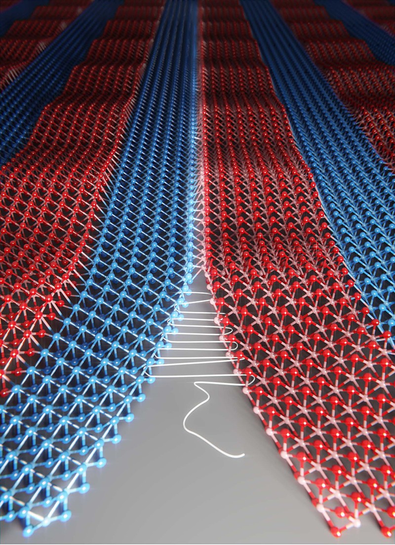
Two patches of crystals are seamlessly "sewn" together to create atomically-thin fabrics.
Joining different kinds of materials can lead to all kinds of breakthroughs. It’s an essential skill that allowed humans to make everything from skyscrapers (by reinforcing concrete with steel) to solar cells (by layering materials to herd electrons).
In electronics, joining different materials produces heterojunctions – the most fundamental components in solar cells, LEDs and computer chips. The smoother the seam between two materials, the more easily electrons flow across it, which is essential for how well electronic devices function. But they’re made up of crystals – rigid lattices of atoms – and they don’t take kindly to being mashed together.
In a study published March 8 in Science, Cornell University and University of Chicago scientists revealed a technique to “sew” two patches of crystals seamlessly together to create atomically thin fabrics.
The team wanted to do this by stitching different fabric-like, three-atom-thick crystals. “Usually these are grown in stages under very different conditions; grow one material first, stop the growth, change the condition, and start it again to grow another material,” said Jiwoong Park, professor of chemistry at the University of Chicago and a senior author on the study.
The resulting single-layer materials are the most perfectly aligned ever grown, according to the researchers. The gentler transition means that at the points where the two lattices meet, one lattice stretches or grows to meet the other – instead of leaving holes or other defects.
“If you think of the materials as two different types of fabric, with two different thread counts, where each row of atoms represents a thread, then we are trying to join them thread-to-thread with no loose threads,” said David A. Muller, Cornell professor of applied and engineering physics and co-director of the Kavli Institute at Cornell for Nanoscale Science, and a senior author on the study. “Using a new type of electron detector – basically a super-fast, super-sensitive camera – we were able to measure the stretching of the materials from where it joined at the atomic scale to how the whole sheet fitted together, and do so with a precision better than one third of one percent of the distance between atoms.”
The atomic seams are so tight, the microscope revealed the larger of the two materials puckers a little around the joint.
“The formation of ripples in these strained 2-D materials provided us with fertile ground for exploring how macroscopic models for the elastic energy can be combined with microscopic theories for the strong underlying van der Waals interactions," said Robert A. DiStasio Jr., assistant professor in Cornell’s Department of Chemistry and Chemical Biology in the College of Arts and Sciences, and one of the paper’s senior authors.
They decided to test its performance in one of the most widely used electronic devices: a diode. Two kinds of material are joined, and electrons are supposed to be able to flow one way through the “fabric,” but not the other.
The diode lit up. “It was exciting to see these three-atom-thick LEDs glowing. We saw excellent performance – the best known for these types of materials,” said Saien Xie, a Cornell graduate student in engineering and first author on the paper.
The discovery opens up some interesting ideas for electronics. Devices like LEDs are currently stacked in layers – 3-D versus 2-D – and are usually on a rigid surface. But the new technique could allow new configurations, like flexible LEDs or atoms-thick 2-D circuits that work horizontally and laterally.
Park noted that the stretching and compressing changed the color of the crystals due to the quantum mechanical effects. This suggests potential for light sensors and LEDs that could be tuned to different colors, for example, or strain-sensing fabrics that change color as they’re stretched.
“This is so unknown that we don’t even know all the possibilities it holds yet,” Park said. “Even two years ago it would have been unimaginable.”
Other coauthors included postdoctoral scholars Kibum Kang, Ka Un Lao and Chibeom Park and graduate students Lijie Tu, Yimo Han, Lujie Huang and Preeti Poddar.
The study received support from the Cornell Center for Materials Research and the Platform for the Accelerated Realization, Analysis and Discovery of Interface Materials at Cornell, the U.S. Air Force Office of Scientific Research, the National Science Foundation and the Samsung Advanced Institute of Technology. Computational resources were provided by the National Energy Research Scientific Computing Center and the Argonne National Laboratory.
Louise Lerner is a writer at the University of Chicago; Linda B. Glaser is a writer for the College of Arts and Sciences.
Media Contact
Get Cornell news delivered right to your inbox.
Subscribe