Nanoscale facility partners with German photonics firm
By Tom Fleischman
The Cornell NanoScale Science and Technology Facility (CNF) has entered into a partnership with the Fraunhofer Institute for Photonic Microsystems (IPMS) in Dresden, Germany, to help small companies accelerate product research and development.
The partners have completed a tool map – a list of tools and fabrication-process steps that both labs support – that allows companies to plan the growth of their R&D prototyping activities by minimizing technology disruptions as they transfer their micro/nanofabrication processes from lab to foundry.
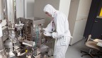
The CNF – an open, multi-user facility operated with funding from the National Science Foundation; Empire State Development Division of Science, Technology and Innovation; and Cornell – is known for its flexible prototyping facilities and engineering support during product R&D. Each year it attracts approximately 600 users, many from outside the university.
CNF now adds the Fraunhofer Institute to its list of partners that can provide a significant commercial ramp-up and volume manufacturing for clients who wish to grow their silicon-related and MEMS (micro-electro-mechanical systems) businesses beyond what CNF can provide.
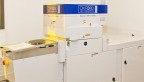
Fraunhofer offers microelectronic R&D and pilot manufacturing tools for various application fields and at institutes across Germany. In this partnership, the CNF-Fraunhofer tool map is focused on silicon-related processes available at Fraunhofer IPMS facilities in Dresden, which will make two clean room facilities available: a 200mm-wafer MEMS clean room and a 300mm-wafer advanced CMOS (complementary metal-oxide-semiconductor) clean room.
“We are excited to have a partner where we can refer our small business customers to get the assistance they need to fully commercialize their concepts and prototypes in the CMOS, silicon photonics and MEMS space,” Don Tennant, CNF director of operations, said in a statement. “We also hope that cross referrals to CNF will allow us to provide services to Fraunhofer clients who are not yet at the scale-up stage and require the flexibility to explore a variety of approaches.”
Martin Landgraf, Fraunhofer IPMS program coordinator, echoed Tennant’s sentiments.
“We are delighted to have this cooperation in place,” he said. “With our recent multi-million-dollar investments in new process equipment and tool upgrades, we have enlarged our wafer processing capacity significantly. … Clients also benefit from our vast experience in lab-to-fab services, our strong network and the quick availability of our semiconductor consumables screening platform capabilities.”
The two sites plan to post the tool map on their customer websites to allow small businesses to plan their path to product introduction earlier in the prototype stages of their work.
Fraunhofer IPMS is part of Fraunhofer-Gesellschaft, the leading organization for applied research in Europe. Its research activities are conducted by 72 institutes and research units at locations throughout Germany.
For more information on this partnership, visit the CNF website or email information@cnf.cornell.edu.
Media Contact
Get Cornell news delivered right to your inbox.
Subscribe