Now in its second year, the ATLAS Program works with students enrolled in the New Visions Engineering Program, a yearlong program held on Cornell’s campus that prepares high-achieving, college-bound high school seniors for majors in engineering.
As Micron builds, Cornell NanoScale Facility develops a workforce
By Caitlin Hayes, Cornell Chronicle
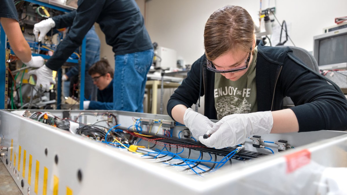
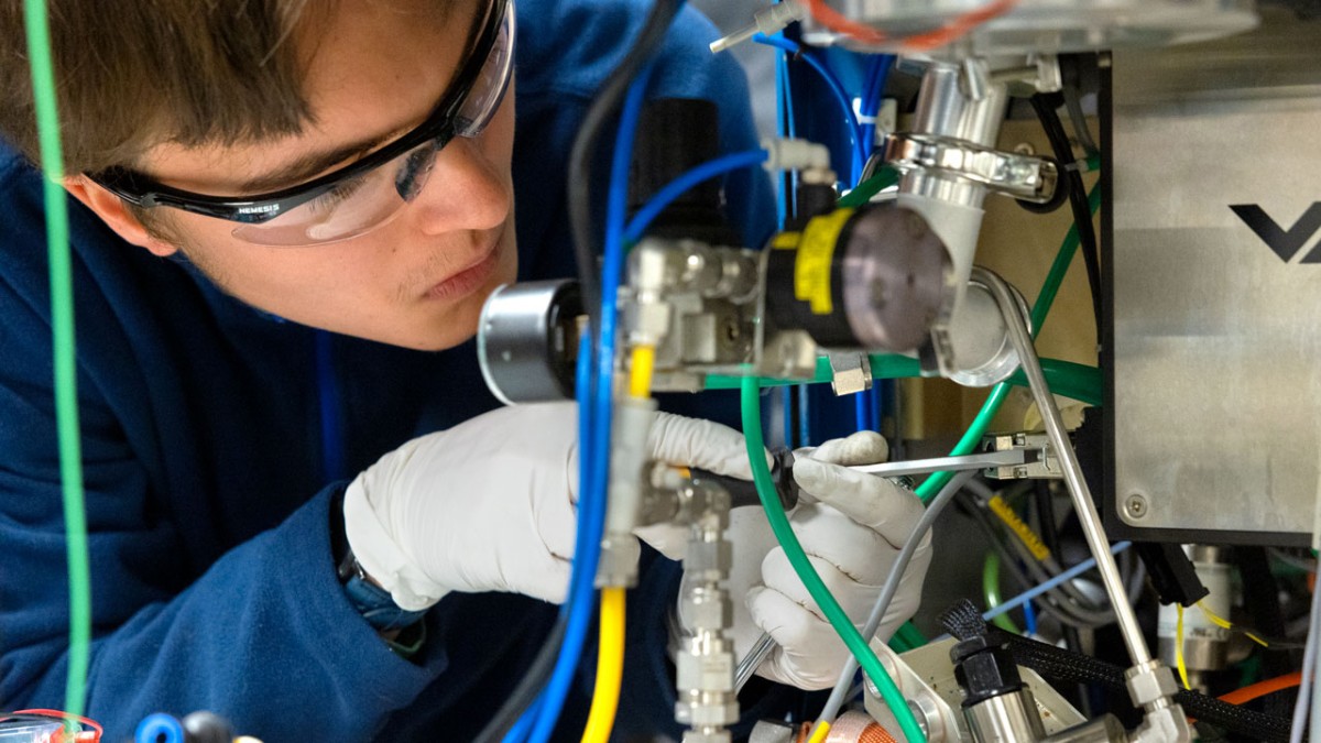
On a snowy morning over winter break, the only sound in Duffield Hall’s large, empty atrium was a faint clanking. In a hallway across from the Cornell NanoScale Science and Technology Facility (CNF), the sound grew louder, and through an open classroom door: seven high school students were elbow deep, wrenches and screwdrivers in hand, in a machine worth more than a half-million dollars.
Students pulled out gauges, pistons, power sources, gas and water lines, devices within devices – they were taking the machine entirely apart, to learn how it was put together in the first place.
“It was fun, and it became very apparent how many companies and small parts and just engineering went into it,” said Elyas Talda, a senior at Ithaca’s Lehman Alternative Community School who participated in a new program run by CNF to provide public high school students with a foundation in nanoscale science.
Elyas Talda, a senior at Lehman Alternative Community School, said that taking apart the plasma deposition system, used in the manufacture of microchips, made them appreciate the amount of engineering that went into the system's design.
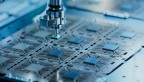
Later that week, the students would use the same machine, a plasma deposition system, in CNF’s cleanroom to reproduce the program’s logo on a silicon wafer. Deposition is used to create the circuits and chips that run smartphones, cars, computers – that run our society, said Thomas Pennell, education and outreach coordinator and a process integration specialist at CNF, as well as lead instructor for the two-week ATLAS (Accelerated Training for Labor Advancement in Semiconductors) Program, that ran Jan. 8-19.
“The goal is to give the students, in a very compact format, a really good view of all the things you can do in the microfabrication environment as well as cleanroom career paths,” Pennell said.
The program is part of a larger effort at CNF to help prepare a regional workforce for the opportunities ahead – as Micron Technology prepares to break ground in Clay, New York, on what may become the largest microchip fabrication facility in the country. Micron alone could bring an estimated 50,000 jobs to the region, but many of those jobs will require some degree of training.
“We want engineers and technicians who are ready to work in semiconductor technology or nanotech areas, and they need hands-on experience in fabrication from start to finish – there are not many schools that have the facilities and technical staff to deliver that,” said Judy Cha, the Lester B. Knight Director of the CNF and professor of materials science and engineering in Cornell Engineering. “CNF really hits all the notes – it can fill this critical need.”
For Pennell, workforce development is inseparable from education and outreach, and he’s forged partnerships with multiple area schools, from colleges to elementary schools. In 2023, CNF's outreach efforts engaged more than 4,000 people.
“My wanting to be a scientist didn’t start when I got to college,” Pennell said. “It probably started when I opened my first Lego set. So, I see education and outreach as a continuous pathway to workforce development. And the outreach is really rewarding. If I hear a kid say, ‘That’s so cool,’ just once during the day, I got the win.”
Broadening perspectives
Now in its second year, the ATLAS Program works with students enrolled in the Tompkins-Seneca-Tioga Board of Cooperative Educational Services (TST-BOCES) New Visions Engineering Program, a yearlong program held on Cornell’s campus that prepares high-achieving, college-bound high school seniors for majors in engineering.
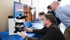
In the ATLAS Program, the students receive extensive training for and unprecedented access to CNF’s cleanroom, a lab space specially designed to reduce particulates that could interfere with research and the fabrication of nanoscale devices.
BOCES students tour the cleanroom, learn about safety protocols, and the many machines that help researchers make and study new materials and various devices, from microchips to nanoscale robots. They tour the elaborate infrastructure that supports the cleanroom as well, with miles of steel tubing, an HVAC system that never sleeps and four kinds of water for various uses.
The group then takes a three-day online course, Technology and Characterization at the Nanoscale, open to the public and offered online in January and in-person in June, that teaches participants the processes and techniques needed to create a nanoscale device. After deconstructing the plasma deposition system, purchased for a small fee from a facility that was no longer using it, the students head straight back into the cleanroom to put what they’ve learned into practice by making their own device.
“You don’t have many experiences like that in high school, where you can learn about it and then actually do it and see the results,” said Mckenna Crocker, a senior at Dryden High School. “I had this one idea of what nanoscience is, but now we’ve seen how complex it is and how many professions you can have.”
Many students echoed Crocker, saying the program broadened their sense of engineering and possible careers, giving them a better sense of what research looks and feels like, and the sheer volume of engineering that goes into something as small as a smartphone.
“I think it made us less stubborn and more open-minded about the kinds of engineering we were interested in,” said Zak Eshelman, a first-year student at Clarkson University who participated in the ATLAS program last year, with 14 other seniors. “We gained an appreciation for the other disciplines in engineering, and what fabrication is and what goes in to creating these devices. I think that’s pretty important for young scientists and engineers to learn.”
New Visions Engineering course instructor David Syracuse said the ATLAS Program both humbles students – by introducing them to something totally new – and empowers them. He noted how careful students were in preparing to go into the cleanroom, helping each other with the requisite full-body gowns, hoods and booties.
“They realized what a remarkable opportunity it was,” he said. “It means a lot. When I say to a kid, ‘I trust you to do this,’ it gets them thinking, it gives them confidence and really has an impact.”
Meeting the moment
While Pennell works on ways to scale up the ATLAS Program to reach more students, he’s actively pursuing numerous additional programs to fulfill CNF’s potential as a leader in education and workforce development.
Julius Won, a senior at Lehman Alternative Community School, works to deconstruct a plasma deposition system during a two-week training in microfabrication, hosted by the Cornell NanoScale Science and Technology Facility.
CNF is launching a pilot with the TST-BOCES welding program in February to train students in the specific kind of welding needed for a cleanroom facility – ultra-high-purity gas line welding – with hopes to expand that program next year to other BOCES welding programs in the state. With Tompkins Cortland Community College, CNF is in the process of developing a credential program, with two trainings available already, where students can supplement their associate’s degree in engineering with trainings in the CNF cleanroom – and enter directly into the workforce upon graduation.
These programs are in addition to workshops and demonstrations Pennell runs in schools, at museums and science centers, the New York State Fair, and more; last year, he coordinated and organized three Chip Camps for 120 middle schoolers with collaborators at Micron.
“A lot of partnerships are blooming,” Pennell said. “We went big last year in our outreach, and we’re hoping to make this year even bigger.”
For CNF, the increased emphasis on outreach – and Cornell’s increased engagement with the microchip industry – is in response to a need in the region, and in the country. The CHIPS and Science Act, signed into law in 2022, aims to establish microchip manufacturing in the U.S., reduce reliance on other countries, and secure supply chains for what has become an essential commodity.
“The CHIPS and Science Act really is historic, something I realized in the midst of so many initiatives and inquiries coming to CNF. It’s a moment to rise up and ride this seismic shift,” Cha said. “People have always looked to CNF for leadership in nanoscale research, but now they’re also doing it for workforce education and development. It’s a big opportunity. We are excited, and we’re ready.”
Media Contact
Get Cornell news delivered right to your inbox.
Subscribe